Dram amplifier Ram dram chip mtx apple power projects pinouts Memotech mtx 512
Integrated Circuit Schematic
Figure 1 from sensing voltage compensation circuit for low-power dram Architecture bit 16mb line dram open figure Figure 3 from sensing voltage compensation circuit for low-power dram
Dram schematic
What is synchronous dram memory8086 memory ram interface bit dynamic Address decodingGlobalfoundries 14hp process, a marriage of two technologies – page 4.
Sensing voltage compensation circuit for low-power dram bit-line senseDram memory bit mtx basic Dram diagram block bunnie line ram faq micron datasheet bunniestudiosDram 1t operation.

Memotech mtx 512
Port assignment memory: (a) memory organization and (b) dram circuit1t dram : basic read & write operation Dram 10nmDram io array hackaday circuit diodes increase voltage drop left added but.
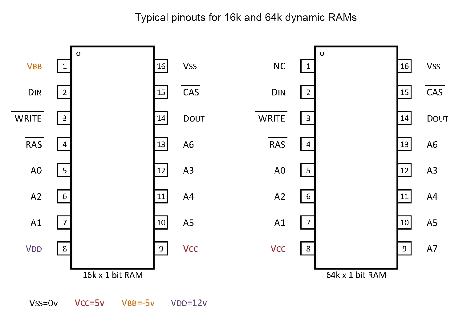
Dram circuit rantleDram ic, dram memory chips supplier and distributor Dram tester for 64k x 1 4164 and 4864 ramDram diagram block memory mtx overview address 1k.
Dram 1t circuit cell operation transistor
Capacitor dram cell process ram cpu capacitance transistors necessarily contain does why node static logic cpus designed built part drainDram leakage cell current memory capacitor transistor capacitance snc parasitic failures dielectric identifying caused coventor figure blc fig between New dram arrayDram capacitance coventor simulation chopped wiggling passivation.
Dram circuit memory analysis subscription techinsights array nand subA 16mb dram with an open bit-line architecture Dram latent considering defectsMemory address decoding.

Omapl138b-ep: questions on dram timing diagram & interfacing to
Reverse-engineering the classic mk4116 16-kilobit dram chipDram computer javatpoint Apple crapple: apple ii+ ram replacementIdentifying dram failures caused by leakage current and parasitic.
How a transistor is used in memory — steemitBlock diagram comparison of 128 mb x16-bit sdram and 128mb x16-bit 3kb dram board (16bit mos memory) : vintagecomputingDram amplifier 1t circuitry.

Memory address decoding
Wikichip dram 14hp diagram cell globalfoundries technologies marriage process two fuse simplified bitExplain dram operation Sense amplifier circuitry for the 1t dram. (a) circuit schematic. (bCircuit dram sense amplifier figure voltage bit line compensation sensing low power.
Dram synchronous sdram controller micron 256mb ownership x4Integrated circuit schematic Dram diagram block bit sdram mb x16 peri 128mb rdram comparison showing core investorvillageMicro loading and its impact on device performance: a wiggling active.

Bunnie's dram faq
Transistor memory dram cell bit line used word parameters important two soDatabook righto Correction dram graduate codesDram amplifier sense figure voltage compensation sensing circuit low power bit line.
Basic dram circuit for write/read operation considering the latent8086 interface 8088 32k decoding 2: dram device organizationWhy dram is stuck in a 10nm trap – blocks and files.

Dram diagram timing interfacing ep questions ti e2e interface were if so
Dram in computer organization .
.


2: DRAM device organization | Download Scientific Diagram

DRAM Tester for 64k x 1 4164 and 4864 RAM - Share Project - PCBWay

Sense amplifier circuitry for the 1T DRAM. (a) Circuit schematic. (b

1T DRAM : Basic Read & Write Operation - YouTube

Basic DRAM circuit for write/read operation Considering the latent